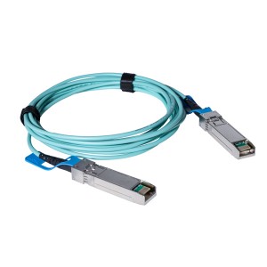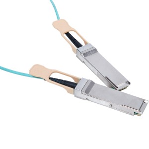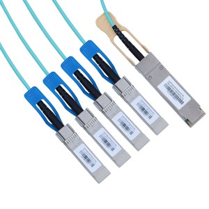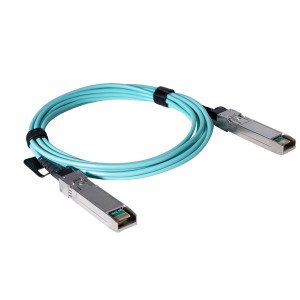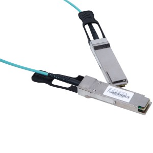
QSFP+/4-SFP+ Active Optical Cables JHA-QSFP-4SFP-40G-AOC
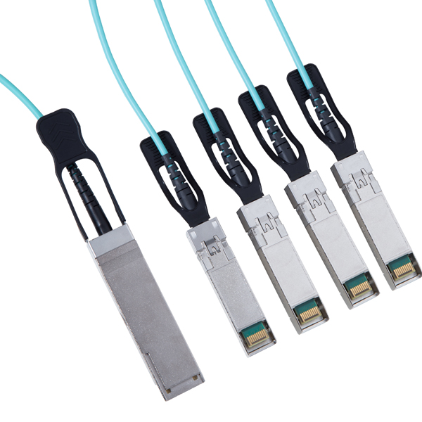
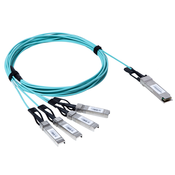
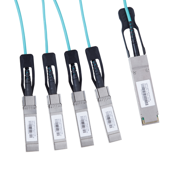
◊ Support 40-4*10GBASE-SR application
◊ Electrical interface compliant to QSFP+ connector (SFF-8436) and SFP+ connector (SFF-8431)
◊ 850nm VCSEL transmitter, PIN photo-detector receiver
◊ Multi rate of up to 10.3125Gbps per lane
◊ Operating case temperature: 0 to 70℃
◊ +3.3V power supply voltage
◊ Low power consumption
◊ RoHS compliant
◊ UL certification cables (optional)
Applications
◊ 40-4*10 Gbe-SR
◊ Fibre Channel Applications
◊ InfiniBand QDR, SDR, DDR
◊ Servers, switches, storage and host card adapters,etc.
Specifications:
Absolute Maximum Ratings
| Parameter | Symbol | Min | Typical | Max | Unit |
| Storage Temperature | TS | -10 | - | +85 | ℃ |
| Operating Humidity | RH | +5 | - | +85 | % |
| Supply Voltage | VCC | -0.5 | +3.3 | +3.6 | V |
Recommended Operating Conditions
|
Parameter |
Symbol |
Min |
Typical |
Max |
Unit |
|
Operating Case Temperature |
TC |
0 |
|
+70 |
℃ |
|
Supply Voltage |
VCC |
+3.14 |
+3.3 |
+3.47 |
V |
|
Supply current (QSFP+) |
ICC |
- |
- |
450 |
mA |
|
Supply current (SFP+)(per terminal) |
|
- |
- |
150 |
mA |
|
Channel Data Rate |
Dr |
|
10.3125 |
- |
Gbps |
|
Fiber bend radius |
- |
3 |
- |
- |
CM |
Electrical and Optical characteristics
Measured condition: Channel Data Rate 10.3125Gbps, VRCCR=3.3V, PRBS31, Case Operating Temperature 0~70℃
Transmitter
| Parameter |
Symbol |
Min |
Typical |
Max |
Unit |
| Centre Wavelength |
λc |
830 |
850 |
870 |
nm |
| RMS spectral width |
Pm |
- |
- |
0.45 |
nm |
| Average launch power, each lane |
PAVG |
-6.0 |
- |
+2.4 |
dBm |
| Extinction Ratio |
ER |
3.0 |
- |
- |
dB |
| Input differential swing |
Vin PP |
200 |
- |
1600 |
mV |
| Input differential impedance |
Zin |
90 |
100 |
110 |
Ω |
Receiver
| Parameter |
Symbol |
Min |
Typical |
Max |
Unit |
| Centre Wavelength |
λc |
830 |
850 |
870 |
nm |
| Bit Error Rate |
BER |
- |
- |
E-12 |
|
| Differential Data Output Swing |
Vout PP |
400 |
- |
1000 |
mV |
| Output Differential Impedance |
Zout |
90 |
100 |
110 |
Ω |
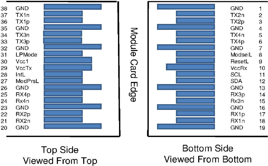
QSFP + Pin Descriptions
|
PIN |
Name |
Function/Description |
|
|
1 |
GND |
Module Ground | |
|
2 |
Tx2n |
Transmitter inverted data input | |
|
3 |
Tx2p |
Transmitter non-inverted data input | |
|
4 |
GND |
Module Ground | |
|
5 |
Tx4n |
Transmitter inverted data input | |
|
6 |
Tx4p |
Transmitter non-inverted data input | |
|
7 |
GND |
Module Ground | |
|
8 |
MODSEIL |
Module Select | |
|
9 |
ResetL |
Module Reset | |
|
10 |
VCCRx |
+3.3v Receiver Power Supply | |
|
11 |
SCL |
2-wire Serial interface clock | |
|
12 |
SDA |
2-wire Serial interface data | |
|
13 |
GND |
Module Ground | |
|
14 |
RX3p |
Receiver non-inverted data output | |
|
15 |
RX3n |
Receiver inverted data output | |
|
16 |
GND |
Transmitter Power Supply | |
|
17 |
RX1p |
Receiver non-inverted data output | |
|
18 |
RX1n |
Receiver inverted data output | |
|
19 |
GND |
Module Ground | |
|
20 |
GND |
Module Ground | |
|
21 |
RX2n |
Receiver inverted data output | |
|
22 |
RX2p |
Receiver non-inverted data output | |
|
23 |
GND |
Module Ground | |
|
24 |
RX4n |
Receiver inverted data output | |
|
25 |
RX4p |
Receiver non-inverted data output | |
|
26 |
GND |
Module Ground | |
|
27 |
ModPrsL |
Module Present, internal pulled down to GND | |
|
28 |
IntL |
Interrupt output, should be pulled up on host board | |
|
29 |
VCCTx |
+3.3v Transmitter Power Supply | |
|
30 |
VCC1 |
+3.3v Power Supply | |
|
31 |
LPMode |
Low Power Mode | |
|
32 |
GND |
Module Ground | |
|
33 |
Tx3p |
Transmitter non-inverted data input | |
|
34 |
Tx3n |
Transmitter inverted data input | |
|
35 |
GND |
Module Ground | |
|
36 |
Tx1p |
Transmitter non-inverted data input | |
|
37 |
Tx1n |
Transmitter inverted data input | |
|
38 |
GND |
Module Ground | |
SFP + Pin Descriptions
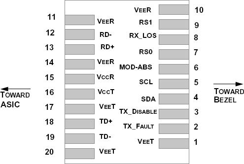
| Pin | Symbol | Name/Description | Notes |
| 1 | VEET | Module Transmitter Ground | 1 |
| 2 | TX_FAULT | Module Transmitter Fault | 2 |
| 3 | TX_DISABLE | Transmitter Disable; Turns off transmitter laser output | 3 |
| 4 | SDA | 2-Wire Serial Interface Data Line (MOD-DEF2) | |
| 5 | SCL | 2-Wire Serial Interface Clock (MOD-DEF1) | |
| 6 | MOD_ABS | Module Absent, connected to VEET or VEER in the module | 2 |
| 7 | RS0 | Rate Select 0, optionally controls SFP+ module receiver | |
| 8 | RX_LOS | Receiver Loss of Signal Indication (In FC designated as Rx_LOS and in Ethernet designated as NOT Signal Detect) | 2 |
| 9 | RS1 | Rate Select 1, optionally controls SFP+ module transmitter | |
| 10 | VEER | Module Receiver Ground | 1 |
| 11 | VEER | Module Receiver Ground | 1 |
| 12 | RD- | Receiver Inverted Data Output | |
| 13 | RD+ | Receiver Non-Inverted Data Output | |
| 14 | VEER | Module Receiver Ground | 1 |
| 15 | VCCR | Module Receiver 3.3 V Supply | |
| 16 | VCCT | Module Transmitter 3.3 V Supply | |
| 17 | VEET | Module Transmitter Ground | 1 |
| 18 | TD+ | Transmitter Non-Inverted Data Input | |
| 19 | TD- | Transmitter Inverted Data Input | |
| 20 | VEET | Module Transmitter Ground | 1 |
Mechanical Design Diagram
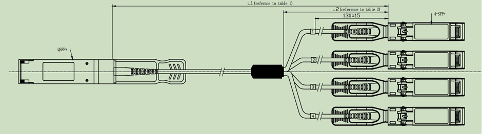 Table 1
|
Cable Length L1(Unit: m) |
Tolerant(Unit: cm) |
|
<1.0 |
+5/-0 |
|
1.0~4.5 |
+15/-0 |
|
5.0~14.5 |
+30/-0 |
|
≥15.0 |
+2%/-0 |
Table 2
|
Length L1(Unit: m) |
Length L2(Unit: m) |
|
1.0 |
0.7 |
|
2 |
1.4 |
|
3 |
2 |
|
≥5.0 |
3 |
Warnings
Handling Precautions: This device is susceptible to damage as a result of electrostatic discharge (ESD).
A static free environment is highly recommended. Follow guidelines according to proper ESD procedures.
Laser Safety: Radiation emitted by laser devices can be dangerous to human eyes. Avoid eye exposure to direct or indirect radiation.