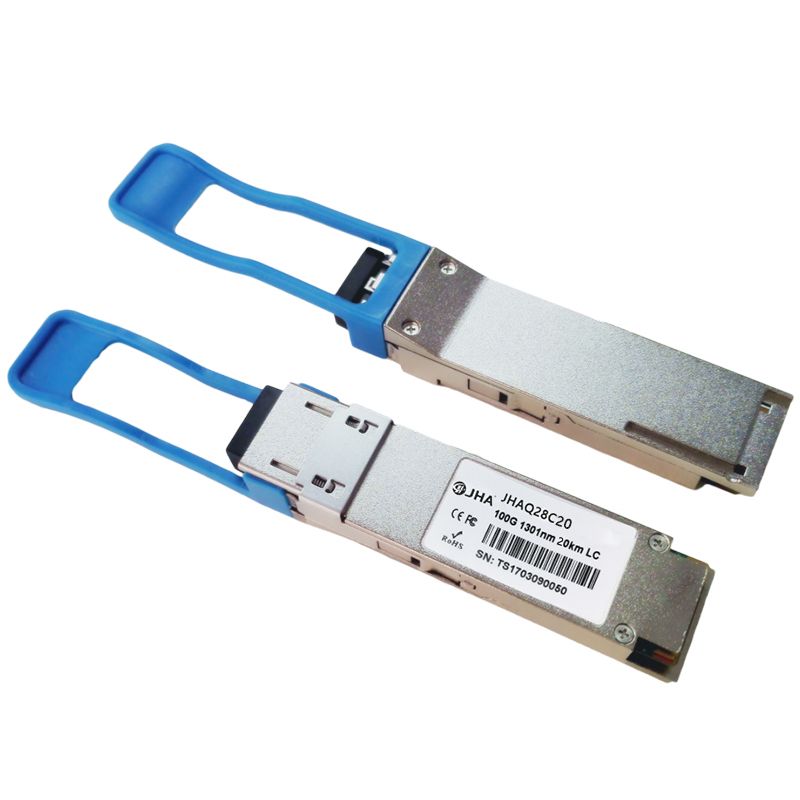
Factory Price 100km SFP - 100Gb/s QSFP28 1310nm 20km LR4 LC Transceiver JHA-Q28C20 – JHA
Factory Price 100km SFP - 100Gb/s QSFP28 1310nm 20km LR4 LC Transceiver JHA-Q28C20 – JHA Detail:
Features:
◊ 4 lanes MUX/DEMUX design
◊ Integrated LAN WDM TOSA / ROSA for up to 20 km reach over SMF
◊ Support 100GBASE-LR4 for line rate of 103.125Gbps and OTU4 for line rate of 111.81Gbps
◊ Aggregate bandwidth of > 100Gbps
◊ Duplex LC connectors
◊ Compliant with IEEE 802.3-2012 Clause 88 standard IEEE 802.3bm CAUI-4 chip to module electrical standard ITU-T G.959.1-2012-02 standard ·
◊ Single +3.3V power supply operating
◊ Built-in digital diagnostic functions
◊ Temperature range 0°C to 70°C
◊ RoHS Compliant Part
◊ Support FEC(Forward Error Correction)
Applications:
◊ Local Area Network (LAN)
◊ Wide Area Network (WAN)
◊ Ethernet switches and router applications
Description:
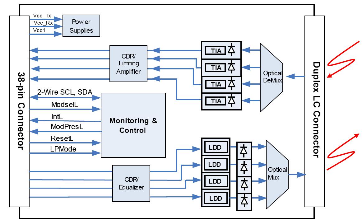
The JHA-Q28C20 is a transceiver module designed for 20km optical communication applications. The design is compliant to 100GbASE-LR4 of the IEEE 802.3-2012 Clause 88 standard IEEE 802.3bm CAUI-4 chip to module electrical standard ITU-T G.959.1-2012-02 standard . The module converts 4 inputs channels (ch) of 25.78 Gbps to 27.95Gbps electrical data to 4 lanes optical signals, and multiplexes them into a single channel for 100Gb/s optical transmission. Reversely, on the receiver side, the module optically de-multiplexes a 100Gb/s input into 4 lanes signals, and converts them to 4 lanes output electrical data.
The central wavelengths of the 4 lanes are 1296 nm, 1300 nm, 1305 nm and 1309 nm . It contains a duplex LC connector for the optical interface and a 38-pin connector for the electrical interface. To minimize the optical dispersion in the long-haul system, single-mode fiber (SMF) has to be applied in this module.
The product is designed with form factor, optical/electrical connection and digital diagnostic interface according to the QSFP28 Multi-Source Agreement (MSA). It has been designed to meet the harshest external operating conditions including temperature, humidity and EMI interference.
The module operates from a single +3.3V power supply and LVCMOS/LVTTL global control signals such as Module Present, Reset, Interrupt and Low Power Mode are available with the modules. A 2-wire serial interface is available to send and receive more complex control signals and to obtain digital diagnostic information. Individual channels can be addressed and unused channels can be shut down for maximum design flexibility.
The JHA-Q28C20 is designed with form factor, optical/electrical connection and digital diagnostic interface according to the QSFP28 Multi-Source Agreement (MSA). It has been designed to meet the harshest external operating conditions including temperature, humidity and EMI interference. The module offers very high functionality and feature integration, accessible via a two-wire serial interface.
• Absolute Maximum Ratings
|
Parameter |
Symbol |
Min. |
Typical |
Max. |
Unit |
| Storage Temperature |
TS |
-40 |
|
+85 |
°C |
| Supply Voltage |
VCCT, R |
-0.5 |
|
4 |
V |
| Relative Humidity |
RH |
0 |
|
85 |
% |
• Recommended Operating Environment:
|
Parameter |
Symbol |
Min. |
Typical |
Max. |
Unit |
| Case operating Temperature |
TC |
0 |
|
+70 |
°C |
| Supply Voltage |
VCCT, R |
+3.13 |
3.3 |
+3.47 |
V |
| Supply Current |
ICC |
|
1100 |
1500 |
mA |
| Power Dissipation |
PD |
|
|
5 |
W |
• Electrical Characteristics (TOP = 0 to 70 °C, VCC = 3.13 to 3.47 Volts
|
Parameter |
Symbol |
Min |
Typ |
Max |
Unit |
Note |
||
| Data Rate per Channel |
|
- |
25.78125 |
|
Gbps |
|
||
|
|
|
27.9525 |
|
|
||||
| Power Consumption |
|
- |
3.6 |
5 |
W |
|
||
| Supply Current |
Icc |
|
1.1 |
1.5 |
A |
|
||
| Control I/O Voltage-High |
VIH |
2.0 |
|
Vcc |
V |
|
||
| Control I/O Voltage-Low |
VIL |
0 |
|
0.7 |
V |
|
||
| Inter-Channel Skew |
TSK |
|
|
35 |
Ps |
|
||
| RESETL Duration |
|
|
10 |
|
Us |
|
||
| RESETL De-assert time |
|
|
|
100 |
ms |
|
||
| Power On Time |
|
|
|
100 |
ms |
|
||
| Transmitter | ||||||||
| Single Ended Output Voltage Tolerance |
|
0.3 |
|
Vcc |
V |
1 |
||
| Common mode Voltage Tolerance |
|
15 |
|
|
mV |
|
||
| Transmit Input Diff Voltage |
VI |
150 |
|
1200 |
mV |
|
||
| Transmit Input Diff Impedance |
ZIN |
85 |
100 |
115 |
|
|
||
| Data Dependent Input Jitter |
DDJ |
|
0.3 |
|
UI |
|
||
| Receiver | ||||||||
| Single Ended Output Voltage Tolerance |
|
0.3 |
|
4 |
V |
|
||
| Rx Output Diff Voltage |
Vo |
370 |
600 |
950 |
mV |
|
||
| Rx Output Rise and Fall Voltage |
Tr/Tf |
|
|
35 |
ps |
1 |
||
| Total Jitter |
TJ |
|
0.3 |
|
UI |
|
||
Note:
- 20~80%
• Optical Parameters(TOP = 0 to 70 °C, VCC = 3.0 to 3.6 Volts)
|
Parameter |
Symbol |
Min |
Typ |
Max |
Unit |
Ref. |
||
| Transmitter | ||||||||
| Wavelength Assignment |
L0 |
1294.53 |
1295.56 |
1296.59 |
nm |
|
||
|
L1 |
1299.02 |
1300.05 |
1301.09 |
nm |
|
|||
|
L2 |
1303.54 |
1304.58 |
1305.63 |
nm |
|
|||
|
L3 |
1308.09 |
1309.14 |
1310.19 |
nm |
|
|||
| Side-mode Suppression Ratio |
SMSR |
30 |
- |
- |
dB |
|
||
| Total Average Launch Power |
PT |
-2 |
- |
8.3 |
dBm |
|
||
| Average Launch Power, each Lane |
|
-1 |
- |
4.5 |
dBm |
|
||
| Difference in Launch Power between any two Lanes (OMA) |
|
- |
- |
6.5 |
dB |
|
||
| Optical Modulation Amplitude, each Lane |
OMA |
-2 |
|
4.5 |
dBm |
|
||
| Launch Power in OMA minus Transmitter and Dispersion Penalty (TDP), each Lane |
|
-1.8 |
- |
|
dBm |
|
||
| TDP, each Lane |
TDP |
|
|
2.2 |
dB |
|
||
| Extinction Ratio |
ER |
4 |
- |
- |
dB |
|||
| Transmitter Eye Mask Definition {X1, X2, X3, Y1, Y2, Y3} |
|
{0.25, 0.4, 0.45, 0.25, 0.28, 0.4} |
|
|||||
| Optical Return Loss Tolerance |
|
- |
- |
20 |
dB |
|
||
| Average Launch Power OFF Transmitter, each Lane |
Poff |
|
|
-30 |
dBm |
|
||
| Relative Intensity Noise |
Rin |
|
|
-128 |
dB/HZ |
1 |
||
| Optical Return Loss Tolerance |
|
- |
- |
12 |
dB |
|
||
| Receiver | ||||||||
| Damage Threshold |
THd |
3.3 |
|
|
dBm |
1 | ||
| Average Power at Receiver Input, each Lane |
R |
-11 |
|
0 |
dBm |
|
||
| RSSI Accuracy |
|
-2 |
|
2 |
dB |
|
||
| Receiver Reflectance |
Rrx |
|
|
-26 |
dB |
|
||
| Receiver Power (OMA), each Lane |
|
- |
- |
3.5 |
dBm |
|
||
| LOS De-Assert |
LOSD |
|
|
-15 |
dBm |
|
||
| LOS Assert |
LOSA |
-25 |
|
|
dBm |
|
||
| LOS Hysteresis |
LOSH |
0.5 |
|
|
dB |
|
||
Note
- 12dB Reflection
• Diagnostic Monitoring Interface
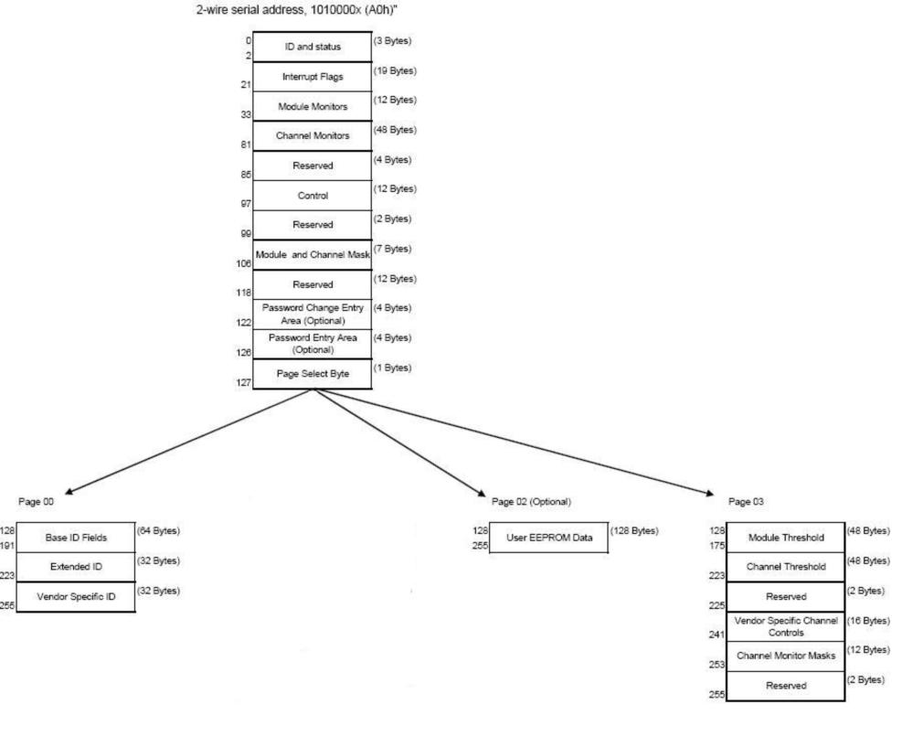
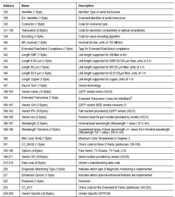
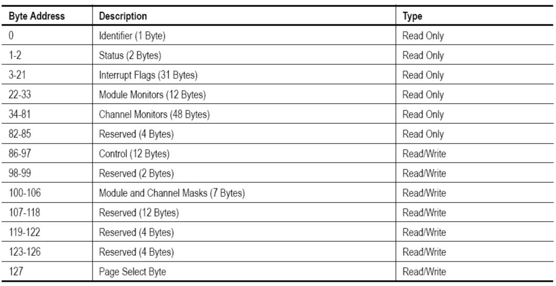
Digital diagnostics monitoring function is available on all QSFP28 LR4. A 2-wire serial interface provides user to contact with module. The structure of the memory is shown in flowing. The memory space is arranged into a lower, single page, address space of 128 bytes and multiple upper address space pages. This structure permits timely access to addresses in the lower page, such as Interrupt Flags and Monitors. Less time critical time entries, such as serial ID information and threshold settings, are available with the Page Select function. The interface address used is A0xh and is mainly used for time critical data like interrupt handling in order to enable a one-time-read for all data related to an interrupt situation. After an interrupt, IntL has been asserted, the host can read out the flag field to determine the affected channel and type of flag.
Page02 is User EEPROM and its format decided by user.
The detail description of low memory and page00.page03 upper memory please see SFF-8436 document.
• Timing for Soft Control and Status Functions
|
Parameter |
Symbol |
Max |
Unit |
Conditions |
| Initialization Time | t_init | 2000 | ms | Time from power on1, hot plug or rising edge of Reset until the module is fully functional2 |
| Reset Init Assert Time | t_reset_init | 2 | μs | A Reset is generated by a low level longer than the minimum reset pulse time present on the ResetL pin. |
| Serial Bus Hardware Ready Time | t_serial | 2000 | ms | Time from power on1 until module responds to data transmission over the 2-wire serial bus |
| Monitor Data ReadyTime | t_data | 2000 | ms | Time from power on1 to data not ready, bit 0 of Byte 2, deasserted and IntL asserted |
| Reset Assert Time | t_reset | 2000 | ms | Time from rising edge on the ResetL pin until the module is fully functional2 |
| LPMode Assert Time | ton_LPMode | 100 | μs | Time from assertion of LPMode (Vin:LPMode =Vih) until module power consumption enters lower Power Level |
| IntL Assert Time | ton_IntL | 200 | ms | Time from occurrence of condition triggering IntL until Vout:IntL = Vol |
| IntL Deassert Time | toff_IntL | 500 | μs | toff_IntL 500 μs Time from clear on read3 operation of associated flag until Vout:IntL = Voh. This includes deassert times for Rx LOS, Tx Fault and other flag bits. |
| Rx LOS Assert Time | ton_los | 100 | ms | Time from Rx LOS state to Rx LOS bit set and IntL asserted |
| Flag Assert Time | ton_flag | 200 | ms | Time from occurrence of condition triggering flag to associated flag bit set and IntL asserted |
| Mask Assert Time | ton_mask | 100 | ms | Time from mask bit set4 until associated IntL assertion is inhibited |
| Mask De-assert Time | toff_mask | 100 | ms | Time from mask bit cleared4 until associated IntlL operation resumes |
| ModSelL Assert Time | ton_ModSelL | 100 | μs | Time from assertion of ModSelL until module responds to data transmission over the 2-wire serial bus |
| ModSelL Deassert Time | toff_ModSelL | 100 | μs | Time from deassertion of ModSelL until the module does not respond to data transmission over the 2-wire serial bus |
| Power_over-ride orPower-set Assert Time | ton_Pdown | 100 | ms | Time from P_Down bit set 4 until module power consumption enters lower Power Level |
| Power_over-ride or Power-set De-assert Time | toff_Pdown | 300 | ms | Time from P_Down bit cleared4 until the module is fully functional3 |
Note:
1. Power on is defined as the instant when supply voltages reach and remain at or above the minimum specified value.
2. Fully functional is defined as IntL asserted due to data not ready bit, bit 0 byte 2 de-asserted.
3. Measured from falling clock edge after stop bit of read transaction.
4. Measured from falling clock edge after stop bit of write transaction.
• Transceiver Block Diagram
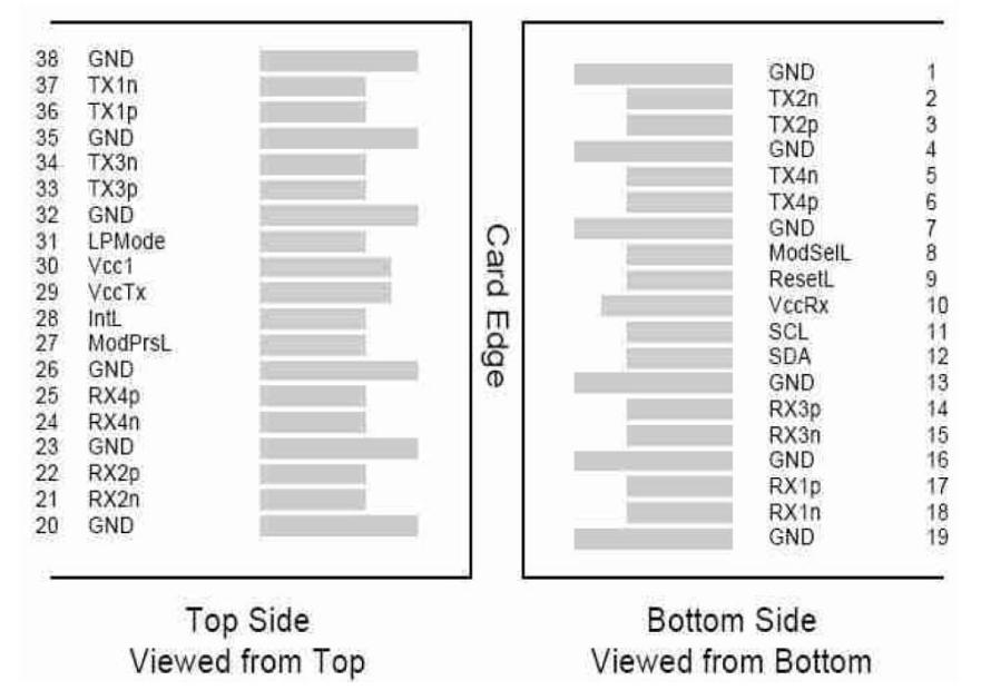
• Pin Assignment
Diagram of Host Board Connector Block Pin Numbers and Name
• Pin Description
|
Pin |
Logic |
Symbol |
Name/Description |
Ref. |
|
1 |
|
GND |
Ground |
1 |
|
2 |
CML-I |
Tx2n |
Transmitter Inverted Data Input |
|
|
3 |
CML-I |
Tx2p |
Transmitter Non-Inverted Data output |
|
|
4 |
|
GND |
Ground |
1 |
|
5 |
CML-I |
Tx4n |
Transmitter Inverted Data Output |
|
|
6 |
CML-I |
Tx4p |
Transmitter Non-Inverted Data Output |
|
|
7 |
|
GND |
Ground |
1 |
|
8 |
LVTTL-I |
ModSelL |
Module Select |
|
|
9 |
LVTTL-I |
ResetL |
Module Reset |
|
|
10 |
|
VccRx |
+3.3V Power Supply Receiver |
2 |
|
11 |
LVCMOS-I/O |
SCL |
2-Wire Serial Interface Clock |
|
|
12 |
LVCMOS-I/O |
SDA |
2-Wire Serial Interface Data |
|
|
13 |
|
GND |
Ground |
1 |
|
14 |
CML-O |
Rx3p |
Receiver Inverted Data Output |
|
|
15 |
CML-O |
Rx3n |
Receiver Non-Inverted Data Output |
|
|
16 |
|
GND |
Ground |
1 |
|
17 |
CML-O |
Rx1p |
Receiver Inverted Data Output |
|
|
18 |
CML-O |
Rx1n |
Receiver Non-Inverted Data Output |
|
|
19 |
|
GND |
Ground |
1 |
|
20 |
|
GND |
Ground |
1 |
|
21 |
CML-O |
Rx2n |
Receiver Inverted Data Output |
|
|
22 |
CML-O |
Rx2p |
Receiver Non-Inverted Data Output |
|
|
23 |
|
GND |
Ground |
1 |
|
24 |
CML-O |
Rx4n |
Receiver Inverted Data Output |
|
|
25 |
CML-O |
Rx4p |
Receiver Non-Inverted Data Output |
|
|
26 |
|
GND |
Ground |
1 |
|
27 |
LVTTL-O |
ModPrsL |
Module Present |
|
|
28 |
LVTTL-O |
IntL |
Interrupt |
|
|
29 |
|
VccTx |
+3.3V Power Supply Transmitter |
2 |
|
30 |
|
Vcc1 |
+3.3V Power Supply |
2 |
|
31 |
LVTTL-I |
LPMode |
Low Power Mode |
|
|
32 |
|
GND |
Ground |
1 |
|
33 |
CML-I |
Tx3p |
Transmitter Inverted Data Output |
|
|
34 |
CML-I |
Tx3n |
Transmitter Non-Inverted Data Output |
|
|
35 |
|
GND |
Ground |
1 |
|
36 |
CML-I |
Tx1p |
Transmitter Inverted Data Output |
|
|
37 |
CML-I |
Tx1n |
Transmitter Non-Inverted Data Output |
|
|
38 |
|
GND |
Ground |
1 |
Notes:
- GND is the symbol for single and supply(power) common for QSFP28 modules, All are common within the QSFP28 module and all module voltages are referenced to this potential otherwise noted. Connect these directly to the host board signal common ground plane. Laser output disabled on TDIS >2.0V or open, enabled on TDIS <0.8V.
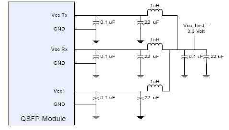
- VccRx, Vcc1 and VccTx are the receiver and transmitter power suppliers and shall be applied concurrently. Recommended host board power supply filtering is shown below. VccRx, Vcc1 and VccTx may be internally connected within the QSFP28 transceiver module in any combination. The connector pins are each rated for maximum current of 500mA.
• Recommended Circuit
• Mechanical Dimensions
Product detail pictures:
Related Product Guide:
With our rich experience and considerate services, we have been recognized as a reliable supplier for many international buyers. Factory Price 100km SFP - 100Gb/s QSFP28 1310nm 20km LR4 LC Transceiver JHA-Q28C20 – JHA , The product will supply to all over the world, such as: Rotterdam, Brisbane, Swiss, More than 26 years, Professional companies from all over the world take us as their long-term and stable partners. We are keeping durable business relationship with more than 200 wholesalers in Japan, Korea, USA, UK, Germany, Canada, France, Italian, Poland, South Africa, Ghana, Nigeria etc.
This enterprise in the industry is strong and competitive, advancing with the times and develop sustainable, we are very pleased to have a opportunity to cooperate!

